
A TVS diode is one stage of a protection circuit, not a complete surge protective device. A selected TVS diode can limit residual voltage at an Ethernet input. Its allowable surge energy depends on the part and test waveform, so exposed-cable designs often coordinate it with a higher-energy stage.
A listed product shows what that looks like. Thor publishes the circuit diagram for the TRSS-RJ45/4 Ethernet surge arrester, and it draws several different kinds of protection element in one device, not one part repeated.
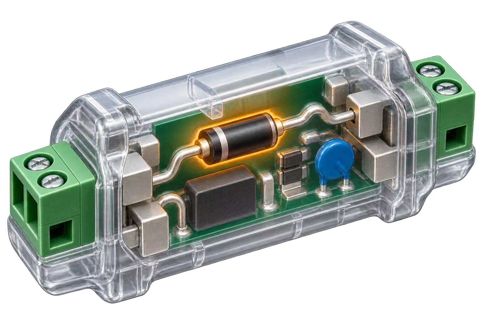
Figure 1 — Conceptual cutaway of a TVS diode as one clamping stage in a generic signal protection module
What a TVS diode actually is
A TVS diode, or transient voltage suppression diode, is a silicon device that stays non-conducting at normal working voltage. When the voltage across it passes its breakdown level it conducts within nanoseconds, clamps the excess, and returns to its blocking state once the transient has gone. Unidirectional parts suit a DC rail with one polarity. Bidirectional parts clamp either polarity, which is what a data pair needs.
That is the whole component. The interesting question is not what it does on its own, but what it is asked to do once it is inside a device alongside a metal oxide varistor or a discharge gap.
Why one component cannot do the whole job
Protecting a data line asks for three things at the same time, and no single part is good at all three.
Energy capability comes first. A surge arriving on a cable run between two buildings carries real energy, and something in the device has to take it. Gap-type components are built for exactly this: they hold off until the voltage reaches their sparkover level, then become a near short circuit and pass current to earth.
The problem is what happens before they fire. A gap does nothing until the voltage across it is high enough, and that sparkover voltage is far above what an Ethernet PHY will survive. Energy capability and a low let-through voltage pull in opposite directions.
A TVS diode solves the second problem and creates a third. It starts conducting close to its rated standoff voltage, so the voltage the protected equipment sees stays low and predictable. Its energy capability is bounded by the die, though, and a transient that exceeds the part rating will destroy it.
The third constraint belongs to data lines specifically. Anything connected across a signal pair adds capacitance, and added capacitance costs bandwidth. A protection design for a 100 Mbps link has to keep insertion loss low enough that the link still closes, which is why a signal SPD datasheet quotes insertion loss and a cut-off frequency at all. A power SPD datasheet has no reason to.
| Element type | Energy capability | Let-through voltage | Effect on a data pair |
| Gap-type, such as a spark gap or gas discharge tube | High | High until it sparks over | Low capacitance, little effect |
| Series element between stages | Not applicable, it decouples | Not applicable | Adds series impedance |
| Semiconductor clamp, such as a TVS diode | Limited by the part rating | Low and closely defined | Adds junction capacitance |
Put those rows next to each other and the design answer writes itself. You use more than one, and you arrange them so each takes the part of the transient it is suited to. The gas discharge tube article covers the first row in more detail.
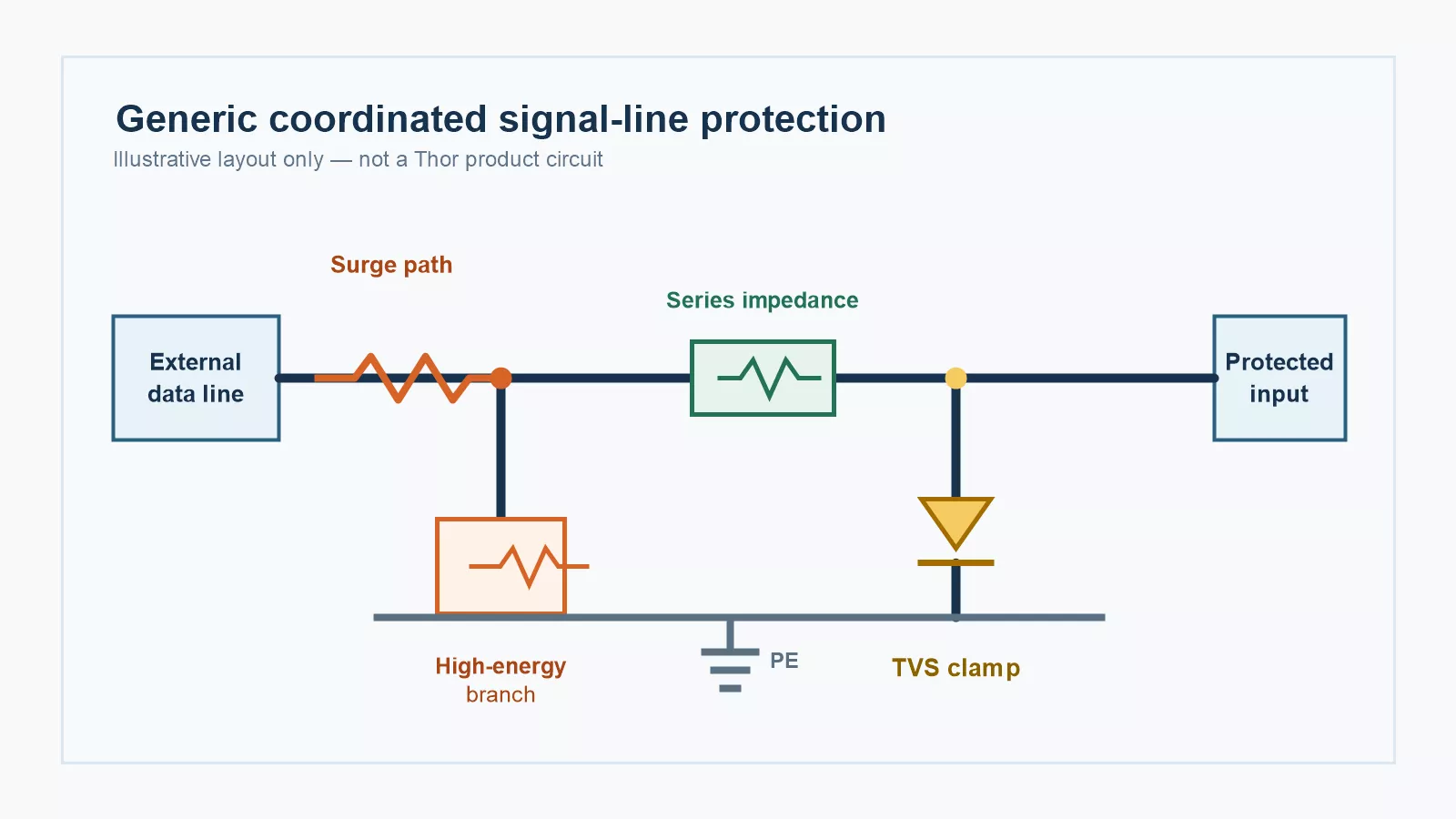
Figure 2 — Generic coordinated signal-line protection with a high-energy branch, series impedance and TVS clamp
What a real signal SPD circuit looks like
Most manufacturers describe their protection circuits in prose. Thor publishes the schematic for the TRSS-RJ45/4, and it is worth looking at for one reason: it settles the question of whether real devices mix element types or pick a favourite.
Three kinds of symbol appear on that drawing. Gap-type symbols, drawn as opposed triangle pairs, appear on one side of the circuit. Elements drawn as a rectangle with a diagonal bridge the protected pairs. Diode branches run from each protected line to a PE busbar, arranged in opposing pairs so that either polarity has a path. Eight pins pass through the device and four of them carry protection elements.
Here is where an honest article has to stop. The drawing carries symbols, not part numbers, and it labels nothing. The gap symbol covers a gas discharge tube and an air gap equally well. The diode symbol covers any diode, and this one carries none of the cathode bend that would mark an avalanche device. Nor does the drawing state a firing sequence, a current split between branches, or which element sets which protection level. Those would be useful things to know, and reading them off an unlabelled schematic would be guesswork dressed up as analysis.
What the drawing does establish is the point of the previous section: a device built for one data line uses at least three different kinds of element, positioned differently. Nobody designing this reached for a single component and scaled it up.
The published ratings are quoted per protection mode, which is the part that affects your specification. The device is rated In 5 kA line to line and In 10 kA line to earth, and its voltage protection level line to earth is 500 V, close to an order of magnitude above the line-to-line figure. Two modes, two sets of numbers. A datasheet that gives one protection level for the whole device is telling you less than this one does, and you should ask why.
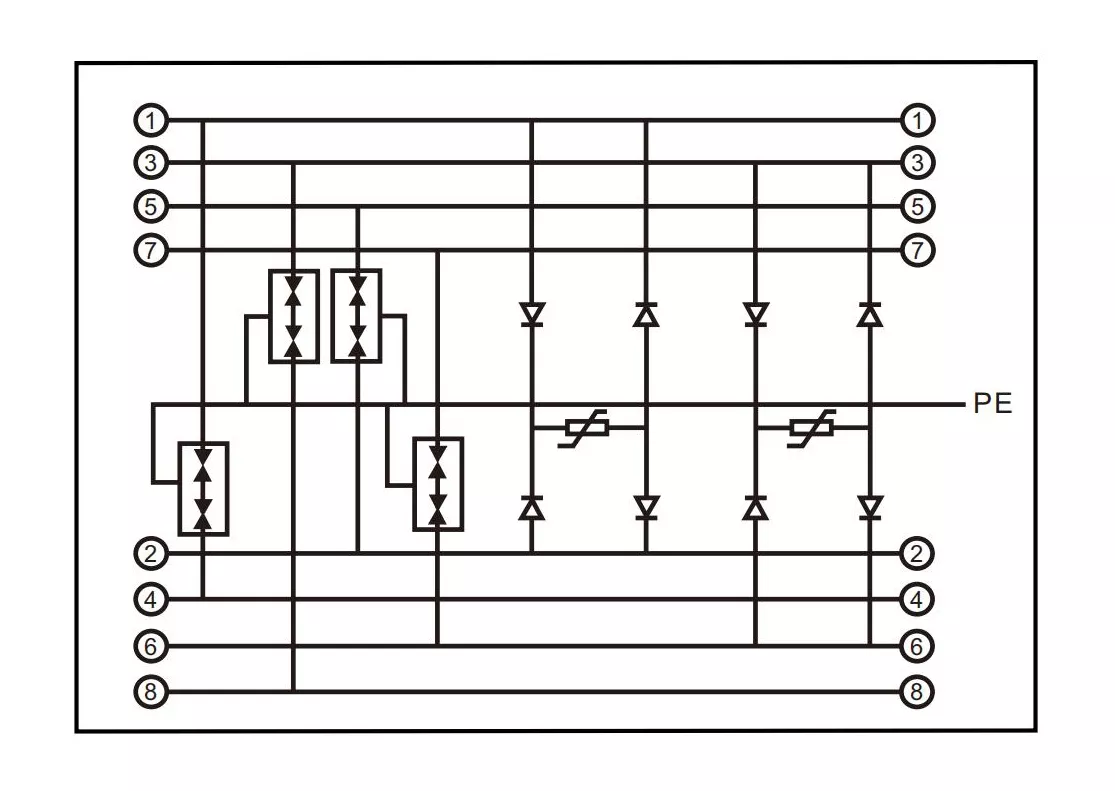
Figure 3 — Published circuit diagram for Thor TRSS-RJ45/4. It shows symbol-level branches, not part numbers or an internal bill of materials.
The pin coverage is worth checking on any RJ45 device before you specify it. The TRSS-RJ45/4 protects four lines, pins 1, 2, 3 and 6, which is PoE Mode A on a 10/100 Mbps link. A gigabit link uses all eight conductors, so it needs an eight-wire model instead. The same staged thinking shows up in the Ethernet and PoE guide, where the working voltages differ but the layered arrangement does not.
Where the power side differs
A distribution board SPD is a different device, and the difference shows up in three measurable places rather than in one headline number.
Rated discharge current is the first. On the 8/20 µs waveform, Thor’s TRSX lightning protection boxes are rated In 10 kA to 50 kA with Imax 20 kA to 100 kA, against 5 kA line to line on the RJ45 device. That is a spread of roughly four to twenty times, depending which models you compare. It is a real gap, and it is smaller than the marketing shorthand about power surges usually suggests.
Second is protection level read against working voltage, not in isolation. Thor’s TRSX-20 lightning protection box is rated Un 380 V AC, and a Up of 1.5 kV on that system sits in a sensible place. So does a Up of 500 V on a 57 V PoE line. Comparing those two numbers directly tells you nothing, because they protect equipment with completely different withstand levels.
Third is the standard. Signal and telecom line SPDs are tested to IEC/EN 61643-21, power system SPDs to IEC/EN 61643-11. Two documents, two test regimes, so the standard must match the circuit being protected.
What does not hold is the tidy story that power SPDs are MOV devices and signal SPDs are semiconductor devices. Thor’s own range breaks it: most AC modules use MOVs, the TRS8-B+C combines an MOV with a GDT, and the TRS-A series uses a graphite gap. Coordinated MOV and TVS designs appear in the research literature as well: D. T. Khanmiri, R. Ball and B. Lehman, “Design of a Hybrid MOV-TVS Diode Surge Protective Device”, 2016 IEEE PES General Meeting, Boston. Staging is the general principle. The component mix follows from the line you are protecting.
Reading the numbers on a signal SPD datasheet
Five fields decide whether a signal SPD suits your line. The rest is packaging.
| Parameter | What it rules out |
| Uc, maximum continuous operating voltage | Any device whose Uc sits below your line’s working voltage, including PoE voltage if the link carries power |
| Up per protection mode | A device whose let-through voltage exceeds what the connected equipment withstands. Check line to line and line to earth separately |
| Insertion loss | A device that loads the pair enough to close your link margin |
| Cut-off frequency | A device with insufficient bandwidth for the data rate, such as a 100 Mbps part on a gigabit link |
| Response time | Rarely a differentiator between comparable devices, and it belongs to the assembled SPD, not to any component inside it |
That last row is worth dwelling on, because response time is quoted more often than it is useful. Thor specifies under 25 ns for the TRSS-RJ45 and also for its MOV-based AC modules. A figure that identical across two very different product lines is not the number that separates them. Insertion loss, bandwidth and the protection level per mode do more work in a real selection.
FAQ
Where should a TVS diode be placed in a protection circuit?
Close enough to the protected input that the clamping voltage seen there, including the voltage developed across the connecting leads, stays inside the equipment’s withstand rating under the surge that installation has to survive. The arrangement follows from that rule. Whether a TVS diode needs a higher-energy stage ahead of it depends on its own pulse rating against the expected surge, on source impedance and line inductance, and on the test condition you are designing to. Exposed external cabling commonly uses coordinated stages because the surge duty is high, while a specified low-energy application can be served by a single part. In a commercial SPD the internal arrangement is the manufacturer’s documented design, and your decision is where the SPD goes, which is covered in SPD coordination.
What causes a TVS diode to fail?
Overstress, meaning a transient beyond the part’s rated peak pulse power or repeated events that accumulate damage. Littelfuse states in its silicon avalanche diode application note that a TVS diode subjected to a transient greater than its datasheet specification will typically fail to a short circuit, which leaves the protected circuit shorted but still protected. At device level, the practical question is how the assembled SPD is specified and replaced; that information belongs on the product documentation rather than in a generic TVS explanation.